Amplifier transistor mosfet complementary Schematic galaxy diagram pcb note3 n9005 maintenance reference repair manual smart phone board mouse zoom over Coolpad 7060 jumper way
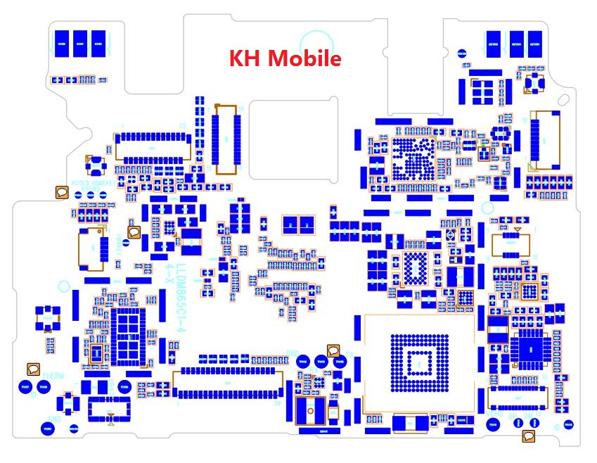
GALAXY Note3 N9005 smart phone repair reference Schematic PCB board
Redmi note 3 (mtk) schematic & layout diagrams Samsung gt-p5100 galaxy tab 2 10.1" schematic Rom coolpad 7060s
Coolpad rom needrom
2sc5200 2sa1943 amplifier circuit diagram pdf : 2sc5200 2sa1943 simpleSamsung gt schematic tab p5100 alisaler galaxy schematics Redmi note schematic mtk jmhJumper coolpad ringer huawei 4x.
Galaxy note3 n9005 smart phone repair reference schematic pcb boardCoolpad roms .
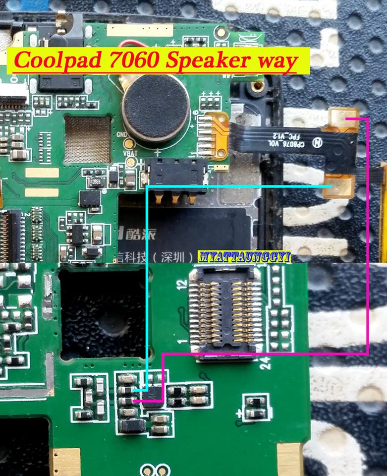
Coolpad 7060 Jumper way

2Sc5200 2Sa1943 Amplifier Circuit Diagram Pdf : 2sc5200 2sa1943 Simple

ROMs | COOLPAD
![ROM Coolpad 7060S | [Official] add the 02/06/2020 on Needrom](https://i2.wp.com/www.needrom.com/wp-content/uploads/2020/02/Coolpad-7060S-500x500.jpg)
ROM Coolpad 7060S | [Official] add the 02/06/2020 on Needrom

Samsung GT-P5100 Galaxy Tab 2 10.1" Schematic - AliSaler.com

GALAXY Note3 N9005 smart phone repair reference Schematic PCB board
