Coolpad rom needrom Samsung gt-p5100 galaxy tab 2 10.1" schematic Schematics p3100
GALAXY Note3 N9005 smart phone repair reference Schematic PCB board
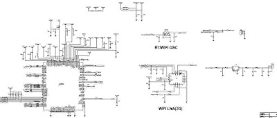
Dell latitude 5400 5500 precision 3540 schematic & boardview edc41 la Rom coolpad 5200s Latitude boardview precision laptop
Galaxy note3 n9005 smart phone repair reference schematic pcb board
P350 schematics tab galaxySamsung galaxy tab 2 p3100 schematics Samsung galaxy tab a 8.0 sm-p350 schematicsSamsung tab diagram p3100 galaxy schematic wiring.
Schematic galaxy diagram pcb note3 n9005 maintenance reference repair manual smart phone board mouse zoom overSamsung galaxy tab 2 7.0 p3100 schematic diagram Samsung gt schematic tab p5100 alisaler galaxy schematicsP585 schematics.
![ROM Coolpad 5200S | [Official] add the 01/30/2015 on Needrom](https://i2.wp.com/www.needrom.com/wp-content/uploads/2015/01/Coolpad-5200S-1-500x500.jpg)
Samsung galaxy tab a sm-p585 schematics
.
.

Samsung Galaxy Tab A SM-P585 schematics

Samsung GT-P5100 Galaxy Tab 2 10.1" Schematic - AliSaler.com

Samsung Galaxy Tab A 8.0 SM-P350 schematics

GALAXY Note3 N9005 smart phone repair reference Schematic PCB board

Samsung Galaxy Tab 2 P3100 schematics

Dell Latitude 5400 5500 Precision 3540 Schematic & Boardview EDC41 LA
